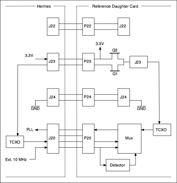
The Hermes Reference Oscillator is roughly grouped into four functional blocks: external reference signal detection, a voltage controlled TCXO, Source Selection and Hermes Interface.
The complete schematics is found here.
External 10 MHz Reference Signal Detection
Instead of requiring a jumper to indicate when an external 10 MHz reference signal is available, the presence of the 10 MHz external reference signal is detected and used to automatically select a reference source.
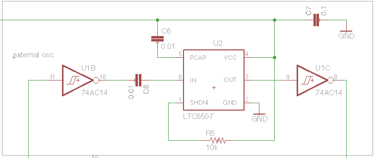
The external 10 MHz signal is first passed through a Schmitt trigger (U1B). The limited signal is detected by an LTC5507 RF detector to provide a somewhat constant output level. This level is further converted into a clean CMOS level by a second Schmitt trigger (U1C).
Voltage Controlled TCXO
Older (pre-2014, approximately) Hermes used a marginally adequate 2.5 ppm TCXO as the internal reference oscillator. Newer Hermes are shipped with an improved 0.1ppm Connor-Winfield TCXO.
The Hermes daughter card includes the voltage controlled version of the 0.1ppm Connor-Winfield TCXO. This permits an older Hermes board to be upgraded to a more stable reference without having to rework the Hermes circuit board itself.
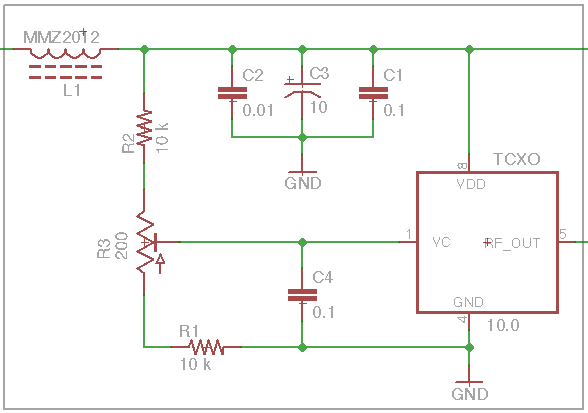
The control input of the voltage controlled TCXO is connected to a voltage divider that is formed by R1, R2 and a trimpot at R3. The TCXO can be periodically calibrated with a reference signal such as WWV to counter any crystal aging (specified to be ± 3ppm or equivalent to ± 30 Hz change at 10 MHz).
Note 3 of the Bill Of Materials (BOM) lists the parts that can be omitted if the calibration function is not required. Without a control voltage, the fixed TCXO should instead be used. The part number of the fixed TCXO is listed in the same note.
Note 1 of the BOM further lists the parts that can be omitted if a replacement TCXO is not required; e.g., if you already have a newer Hermes and do not need the calibration feature.
Source Selection and Hermes Interface
The Hermes Reference daughter card is installed over jumpers J20, J22, J23 and J24 on the Hermes board. These Hermes jumpers are connected to the daughter card through board sockets P20, P22, P23 and P24 on the daughter card.
J22 and J24 on Hermes are used to configure the input termination for the 10 MHz reference input port. Since the original jumpers are obscured by the daughter card, they are replicated as a duplicate set of jumpers on the daughter card. J22 and J24 on the daughter card are simply tied to P22 and P24, which in turn are connected to Hermes' J22 and J24.
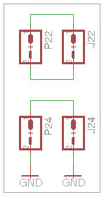
P24 also functions as the ground reference for the daughter card.
J22 and J24 on the daughter card continues to function like the original J22 and J24 on Hermes. J24 provides a ground path for the shell of the 10 MHz External Reference SMA connector (J25) on Hermes, and J22 determines if the external reference is terminated with 50 ohms.
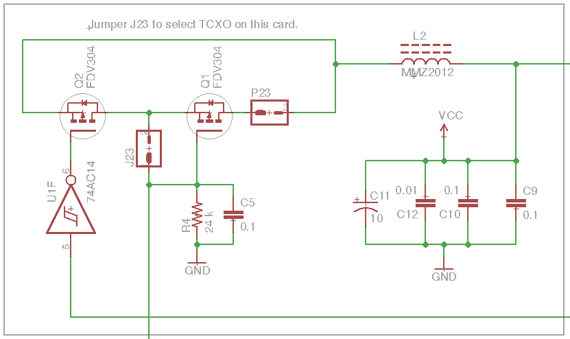
J23 on the Hermes board was used to disconnect power from the internal TCXO, making 3.3V available on P23 to power the components on the daughter card. The 3.3V line is filtered through a ferrite bead chip L2 (MMZ2012R601A) before it is used as VCC by the logic chips. We shall see later that the TCXO has its own set of filters, made up of C1, C2, C3 and L1.
The input of the 74AC14 (U1F) comes from the external 10 MHz reference signal detector. When the external reference is detected, the P-channel MOSFET Q2 (FDV304P) is turned off, severing the power to both the TCXO on the daughter card (through jumper J23) and the TCXO on the Hermes board (through transistor switch Q2).
The 3.3V supply to the daughter card's TCXO is taken from pin 1 of J23. Install a jumper on J23 if you include a TCXO on the daughter card. J23 can be omitted and permanently shorted by a wire during construction, but that comes with a loss of ability to later reconfigure the daughter card to use the old Hermes TXCO in case the daughter card's TCXO suffers a failure. If you decide to omit J23, you might as well also omit Q1.
Q1's gate senses if J23 is installed. If J23 is installed, Q1 is permanently turned off, severing the 3.3V that goes to pin 1 of P23 which feeds power to the original Hermes TCXO.
J20 is used on Hermes to select between the internal TCXO and the external 10 MHz reference signal. We relay these signals up to the daughter card through P20. However all signal paths are now switched by gates and multiplexers instead of routing signals through jumpers.
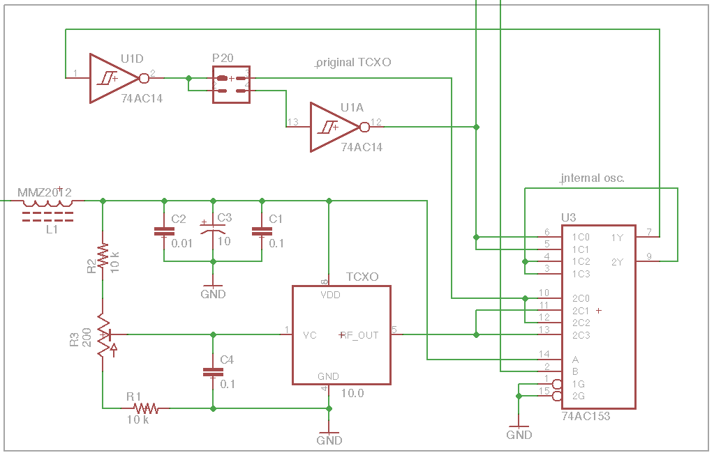
Pin 3 of P20 carries the original TCXO from Hermes. When power is applied to the TCXO through J23, it asserts the least significant address of the multiplexer at U3 (74AC153). This causes the second section of U3 to choose the RF OUT from the daughter card's TCXO instead of the Hermes TCXO, regardless of the state of the most significant address of the multiplexer .
Pin 4 of P20 carries the output of the 10 MHz external reference buffer on Hermes. Since the waveform from the Hermes reference buffer has always been problematical, it is immediately rebuffered by a Schmitt trigger (U1A) before it is used anywhere else.
After the second section of the multiplexer has selected between the two TCXOs, its output (2Y, pin 9 of U3) is fed back to the first section of the multiplexer. The first section of the multiplexer chooses between an internal TCXO and the rebuffered 10 MHz external reference. The selection is chosen by the most significant address of the multiplexer, which comes from the LTC5507 signal detector.
Block Diagram
The following shows a simple block diagram outlining what was described above.